- 您现在的位置:买卖IC网 > Sheet目录1995 > HI5741BIBZ (Intersil)DAC 14BIT 100MHZ 5.2V 28-SOIC
8
FN4071.12
September 20, 2006
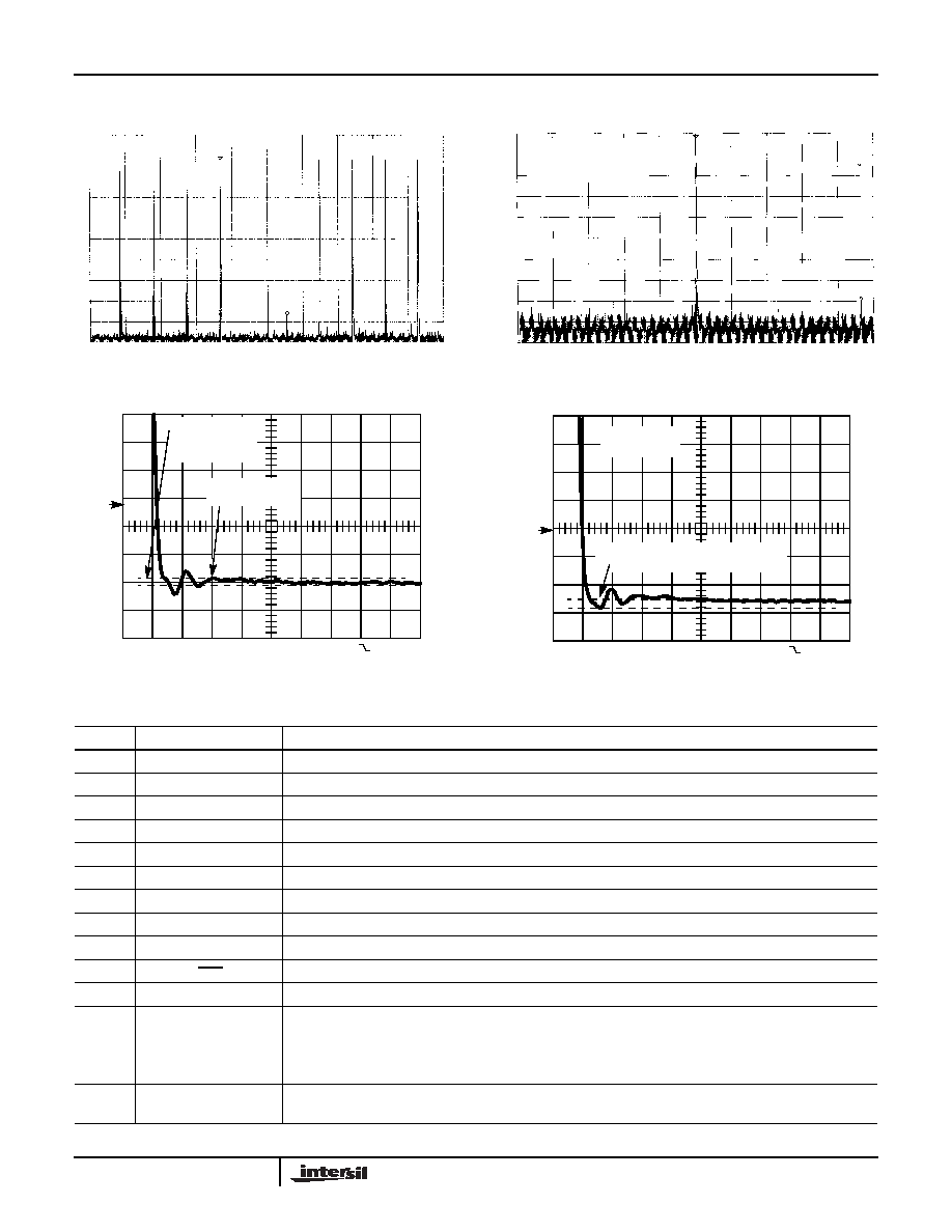
FIGURE 16. TYPICAL MTPR PERFORMANCE
FIGURE 17. SFDR WITHIN A WINDOW
FIGURE 18. TYPICAL SETTLING TIME PERFORMANCE
FIGURE 19. TYPICAL GLITCH ENERGY
Pin Descriptions
PIN NO.
PIN NAME
PIN DESCRIPTION
1-14
D13 (MSB) thru D0 (LSB) Digital Data Bit 13, the Most Significant Bit through Digital Data Bit 0, the Least Significant Bit.
15
CLK
Data Clock Pin 100kHz to 100 MSPS.
16
DVCC
Digital Logic Supply +5V.
17, 28
DGND
Digital Ground.
18
DVEE
-5.2V Logic Supply.
23
RSET
External Resistor to set the full scale output current. IFS = 16 x (VREFOUT/RSET). Typically 976.
27
AGND
Analog Ground Supply current return pin.
19
ARTN
Analog Signal Return for the R/2R ladder.
21
IOUT
Current Output Pin.
20
IOUT
Complementary Current Output pin.
22
AVEE
-5.2V Analog Supply.
24
CTRL AMP IN
Input to the current source base rail. Typically connected to CTRL AMP OUT and a 0.1
F capacitor to AVEE.
Allows external control of the current sources.
25
CTRL AMP OUT
Control amplifier out. Provides precision control of the current sources when connected to CTRL AMP IN
such that IFS = 16 x (VREFOUT/RSET).
26
REF OUT
-1.23V (typical) bandgap reference voltage output. Can sink up to 500
A or be overdriven by an external
reference capable of delivering up to 2mA.
Typical Performance Curves (Continued)
START 1.900MHz
S
STOP 3.100MHz
10dB/
C
fCLK = 20 MSPS
MTPR = 75.17dBc
CENTER 26.637MHz
S
SPAN 2.000MHz
10dB/
C
fCLK = 100 MSPS
fOUT = 26.6MHz
SFDR = 77.5dBc
1
CH1 1.00mV
~
M 5.0ns CH1
-16.9mV
SETTLING TIME
~10ns
: 240V
@: -30.96mV
12-BIT WINDOW
1
CH1 1.00mV
M 5.0ns CH1
-109mV
GLITCH = (0.5) (300
V) (3.3ns)
= 0.495pV/s
: 300V
@: -124.1mV
HI5741
发布紧急采购,3分钟左右您将得到回复。
相关PDF资料
HI5746KCB-T
CONV A/D 10BIT 40MSPS 28-SOIC
HI5760BIBZ
CONV D/A 10-BIT 125MSPS 28-SOIC
HI5762/6IN
CONV A/DDUAL 10BIT 60MSPS 44MQFP
HI5766KCB
CONV A/D 10BIT 60MSPS 28-SOIC
HI5767/6IB
CONV A/D 10BIT 60MSPS 28-SOIC
HI5805BIB
IC ADC 12-BIT 5MSPS 28-SOIC
HI5812JIBZ-T
ADC 12BIT SAMPL TRK&HOLD 24-SOIC
HI5828IN
DAC DUAL 12BIT 130MHZ 48-LQFP
相关代理商/技术参数
HI5741BIBZ-T
功能描述:数模转换器- DAC HI5741BIB IN TAPE RoHS:否 制造商:Texas Instruments 转换器数量:1 DAC 输出端数量:1 转换速率:2 MSPs 分辨率:16 bit 接口类型:QSPI, SPI, Serial (3-Wire, Microwire) 稳定时间:1 us 最大工作温度:+ 85 C 安装风格:SMD/SMT 封装 / 箱体:SOIC-14 封装:Tube
HI5741BIP
制造商:Rochester Electronics LLC 功能描述:28 PDIP INDTEMP D/A 14 BIT 100 MHZ -5.2V - Bulk 制造商:Harris Corporation 功能描述: 制造商:Intersil Corporation 功能描述:
HI5741BIPS2503
制造商:Rochester Electronics LLC 功能描述:- Bulk
HI5741D DIE
制造商:Harris Corporation 功能描述:
HI5741-EVS
功能描述:数据转换 IC 开发工具 HI5741 EVAL PL ATFORM
RoHS:否 制造商:Texas Instruments 产品:Demonstration Kits 类型:ADC 工具用于评估:ADS130E08 接口类型:SPI 工作电源电压:- 6 V to + 6 V
HI5746
制造商:INTERSIL 制造商全称:Intersil Corporation 功能描述:10-Bit, 40 MSPS A/D Converter
HI5746_04
制造商:INTERSIL 制造商全称:Intersil Corporation 功能描述:10-Bit, 40MSPS A/D Converter
HI5746EVAL1
功能描述:EVALUATION PLATFORM HI5746 RoHS:否 类别:编程器,开发系统 >> 过时/停产零件编号 系列:- 标准包装:1 系列:- 传感器类型:CMOS 成像,彩色(RGB) 传感范围:WVGA 接口:I²C 灵敏度:60 fps 电源电压:5.7 V ~ 6.3 V 嵌入式:否 已供物品:成像器板 已用 IC / 零件:KAC-00401 相关产品:4H2099-ND - SENSOR IMAGE WVGA COLOR 48-PQFP4H2094-ND - SENSOR IMAGE WVGA MONO 48-PQFP